
One of the many outrageous old machines hanging around Marlboro's science building is a TSM-91-A analog tritium monitor made by Atomic Accessories Inc.. The goal of this project was to devise a way to turn the monitor into a random number generator, using only a few analog components.
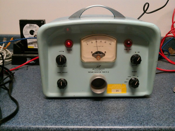
The first challenge was getting a signal out of the monitor. I figured the easiest way to do this was to simply use the signal driving the panel meter, which ended up simply being a voltage from 0-100mV.

In order to retrieve data from the panel meter, the first thing I needed to do was to amplify the small signal. To do this, I turned to the standard inverting amplifier:
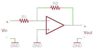
This circuit uses an op-amp in closed-loop configuration, meaning there is negative feedback applied to the inverting input, in this case through R2. In open-loop configuration, that is without negative feedback, the output of the amplifier is given by: \[Vout = A (v^+ - v^-)\] Where \(v^+\) and \(v^-\) are the non-inverting and inverting inputs respectively, and \(A\) is a large gain factor, generally at least in the range of \(10^4\), depending on the specific op-amp. Because of the extremely high gain, op-amps in open-loop configuration are not useful for most applications. In closed-loop configuration, however, the gain may be precisely controlled by external components. There are two important properties of the ideal op-amp which are used in the analysis of closed-loop op-amp circuits. Given the op-amp (assuming a negative-feedback loop in the circuit, though one is not shown):
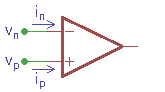
Where \(v_n\) and \(v_p\) are the voltages at the inputs and \(i_n\) and \(i_p\) are the currents flowing into the inputs, we have the two properties: \[v_n = v_p \] \[i_n = i_p = 0\]
With this we can easily analyze the above inverting amplifier circuit. First of all, since \(v_p = v_n\), and it is clear that \(vp=0\), we know that \(v_n=0\). Next we apply Kirchoff's Current Law to the inverting input:
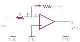
\[i_{R1} + i_{R2} + i_n = 0\] And since we know that \(i_n = 0\): \[i_{R2} = -i_{R1}\] Now we simply solve for \(Vout\) using \(V = I R\): \[i_{R1} = \frac{v_n - Vin}{R1}\] \[i_{R2} = \frac{v_n - Vout}{R2}\] \[\frac{v_n - Vout}{R2} = -\frac{v_n - Vin}{R1}\] \[v_n - Vout= -\frac{R2 (v_n - Vin)}{R1}\] Where \(v_n\) is the voltage at the negative input, and since we know that \(v_n=0\): \[Vout= -\frac{R2}{R1} Vin\] Well that's great when using a dual power supply, but to keep my circuit simple I wanted to use a single supply of 5V. With the above amplifier running off a single supply, the 0-100mV signal would result in the output just sitting at 0V, which wouldn't be very helpful. An easy way to make the inverting amplifier work for single supply circuits is to bias it, by keeping the non-inverting input at some positive voltage:
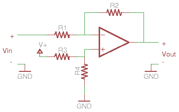
Where \(V^+\) is the power supply. Since there are now two supplies, this circuit is a bit more work to analyze, but can easily be done using the superposition theorem. First, looking at the circuit with \(V^+\) shorted to ground, we can see that \(v_n=0\), and the result is the same as the unbiased amplifier: \[Vout_A = -\frac{R2}{R1} Vin\] Now, with \(Vin\) shorted to ground, we can see that \(v_p\) is the output of a voltage divider, so its value is: \[v_p = \frac{R4}{R3+R4} V^+\] Also notice that, since we've set \(Vin = 0\), \(R1\) and \(R2\) form a voltage divider between \(Vout\) and \(v_n\), so: \[v_n = \frac{R1}{R1+R2} Vout\] Since \(v_n = v_p\), and we know \(v_p\): And since \(v_n = v_p\): \[\frac{R1}{R1+R2} Vout_B = \frac{R4}{R3+R4} V^+\] Which can be simplified to: \[Vout_B = \frac{1 + R2/R1}{1 + R3/R4} V^+\] By the superposition theorem, the actual response of the circuit is the sum of the two: \[Vout = Vout_A + Vout_B\] \[Vout = \frac{1 + R2/R1}{1 + R3/R4} V^+ -\frac{R2}{R1} Vin\] At this point it was time to decide on some real numbers. I decided on the LM358 dual op-amp, as it is low cost and made to run off single rail power supplies. Real op-amp have a property that must be taken into account, wich is their saturation level. In the case of the LM358, the saturation region is entered at \(V^+ - 1.5V\), so having decided on a 5V supply, I knew that the bias and gain had to be such that the calculated output voltage given the maximum input of 100mV would be below 3.5V. I decided I'd bias the signal at \(V^+/2\), with a gain of 10. For the gain: \[\frac{R2}{R1} = 10\] Choosing a nice value for R1 of \(10k\Omega\), we find that \(R2=100k\Omega\). For the bias of \(V^+/2\) we have: \[\frac{1 + R2/R1}{1 + R3/R4} = \frac{1}{2}\] \[\frac{11}{1 + R3/R4} = \frac{1}{2}\] \[R3/R4 = 21\] Choosing \(R4=10k\Omega\) makes \(R3 = 210k\Omega\). Running the simulator on this circuit at CircuitLab, we can see that it behaves as expected:

Now that I had a more usable signal, I had to figure out what to do with it. Since the LM358 has two op-amps, I decided I would come up with a way to use only a single IC, which meant I had one op-amp stage left. Since the monitor has a calibration potentiometer as well as a scale selector switch, I knew that the baseline voltage was fairly arbitrary, so a comparator would not do the trick. The information I was after was the sudden spikes and dips in the signal, independent of the baseline DC component, in other words the derivative of the input signal. Enter the differentiator:
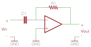
This can be analyzed in the same way as the inverting amplifier: \[i_{R1} = -i_{C1}\] \[i_{C1} = C1 \frac{d}{dt} Vin(t)\] \[i_{R1} = -\frac{Vout}{R1}\] \[\frac{Vout}{R1} = - C1 \frac{d}{dt} Vin(t)\] \[Vout= - C1 R1 \frac{d}{dt} Vin(t)\] And once again, the op-amp is running on a single supply. In this case that means that this circuit will have the desired effect of the output going up when the input goes down quickly, which, since the amplifier is inverting, would mean a spike in the original signal, but it will stay at 0V the rest of the time. Since I also want to know when the input signal drops quickly, this circuit will need to be biased as well:

Like the biased amplifier this can be analyzed by superposition, and it is easy to see that, in the case of \(V^+ = 0\), the output is the same as the unbiased differentiator: \[Vout_A = - C1 R1 \frac{d}{dt} Vin(t)\] And when the \(Vin = 0V\): \[v_p = \frac{R3}{R2+R3} V^+ = v_n\] \[i_{C1} = C1 \frac{d}{dt} v_n(t)\] Since \(V+\) is a constant: \[\frac{d}{dt} v_n(t) = 0\] \[i_{C1} = 0\] Which means that all the current from \(v_n\) is flowing through R1, so: \[Vout_B = \frac{R3}{R2+R3} V^+\] \[Vout = \frac{R3}{R2+R3} V^+ - C1 R1 \frac{d}{dt} Vin(t)\] Once again it's time to make some choices. In this case, a bias of \(V^+/2\) is easily achieved by choosing R2 and R3 equal, so I decided to go with \(10k\Omega\) for both. At this point I have a signal that hovers at 2.5V when the radiation level is steady, goes up when there is a sudden spike in radiation, and goes down when there is a sudden dip. Since this is a ternary output, I might as well make it discrete. This is easily done by setting the gain high enough that the op-amp will be in saturation during the high state, and at 0V during the low state. To stick with nice values here, I decided on \(C1 = 1\mu F\) and \(R1 = 100k\Omega\), giving a gain of 100,000. Again, a quick simulation on CircuitLab reveals that it is doing what it's supposed to:

So the entire circuit is this (C1 is mislabeled as \(1F\), should be \(1\mu F\)):
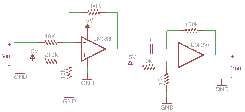
and its total response is given by the composition of the two sub-circuits: \[ Vout = 2.5V - 10^5 \frac{d}{dt} (2.5V - 10 Vin(t)) \] \[ = 2.5V + 10^6 \frac{d}{dt} Vin(t)\] Here's a CircuitLab simulation of the final circuit:
