knob
This section covers the process of setting and reading an analog pin.
Reading an Analog pin
To take an 'analog' reading on the ATtiny85, we can't just take an instantaneous voltage. That's where the Analog to Digital Converter comes in.
As the ADC is a multi-stage, complex process, I will only go into fuzzy detail. If you really want to know what's going on behind the scenes, try to read through most if not all of section 17 roughly from page 126-141.
Let's take a look at an analog read function that I've made:
(if the comments are wrapping around too much, zoom out in the browser. The comments in the actual file are just the stuff on the left of the vertical line of comments.)
int analog_read(int read_pin){
  //Read ADC2L:
  if(read_pin != 1 && read_pin != 2 && read_pin != 3){
    //pin 1 is technically an ADC input but it is also the RESET pin
    //so we pretend it doesn't exist.
    //if read_pin is not a valid number, break.
    return 0;
  }
  ADMUX |= read_pin; //set the pin that the adc reads to ADC2 (PB4) //set which pin on which the ADC will start.
  ADCSRA |= (1 << ADEN); // Analog-Digital enable bit               //start the overall ADC system
                                                                    //this must be enabled before anything can be read.
  ADCSRA |= (1 << ADSC); // Discard first conversion                //the first reading is not reliable so we discard it.
  while (ADCSRA & (1 << ADSC)); // wait until conversion is done    //the ADC conversion takes a certain number of clock cycles (25?)
  ADCSRA |= (1 << ADSC); // start single conversion                 //start a second conversion
  while (ADCSRA & (1 << ADSC)) // wait until conversion is done     //sit in a while loop until that conversion finishes (not very long)
  ADCSRA &= ~(1<<ADEN); // shut down the ADC                        //shut down the ADC to conserve power.
  int low_val = ADCL;                                               //the value from the conversion is stored in ADCH and ADCL.
  int high_val = ADCH;                                              //we combine together the 2 lowest bits of ADCH and the 8 bits of ADCL to get
                                                                    // 10 bit resolution (a number from 0-1023)
  int val = (high_val<<8)|low_val;                                  //the combination of ADCH and ADCL happens here
  //Clear bottom 3 bits of ADMUX:                                   //clear out bottom bits of ADMUX so it doesn't get confused the next time around.
  ADMUX &= ~(0x111);                                                //
  return val;                                                       //return the value of ADCH and ADCL combined (a number from 0-1023)
}
Now that we have a rough understanding of analog_read(), let's see it in action.
Code
Controls the frequency at which an LED blinks based on the position of the knob.
// Define clock speed for delay.h:
// (8MHz internal crystal; /8 prescaler):
#define F_CPU 1000000L

#include <avr/io.h>
#include <util/delay.h>

#define LED1 PB0
#define KNOB PB2

int analog_read(int read_pin){
  //Read ADC2L:
  if(read_pin != 1 && read_pin != 2 && read_pin != 3){
    //if read_pin is not a valid number, break.
    return 0;
  }
  ADMUX |= read_pin; //set the pin that the adc reads to ADC2 (PB4)
  ADCSRA |= (1 << ADEN); // Analog-Digital enable bit
  ADCSRA |= (1 << ADSC); // Discard first conversion
  while (ADCSRA & (1 << ADSC)); // wait until conversion is done
  ADCSRA |= (1 << ADSC); // start single conversion
  while (ADCSRA & (1 << ADSC)) // wait until conversion is done
  ADCSRA &= ~(1<<ADEN); // shut down the ADC
  int low_val = ADCL;
  int high_val = ADCH;
  int val = (high_val<<8)|low_val;
  //Clear bottom 3 bits of ADMUX:
  ADMUX &= ~(0x111);
  return val;
}


void delay_microseconds(int us){
  int i;
  for (i = 0; i < us; i++){
    _delay_us(1);
  }
}

void delay(int ms) {
  int i;
  for (i=0; i<ms; i++) {
    _delay_ms(1);
  }
}

void toggle(int pin){
  PORTB ^= (1<<pin);
}

void set_high(int pin){
  PORTB |= (1<<pin);
}

void set_low(int pin){
  PORTB &= ~(1<<pin);
}

int main(void){
  // Setup :
  //Set LED as output:
  DDRB |= (1<<LED1);
  set_high(LED1); //default is input, 1 is output.
  // Main:
  int knob_pos;
  while (1) {
    knob_pos = analog_read(2);
    delay(knob_pos);
    toggle(LED1);
  }
  return 0;
}
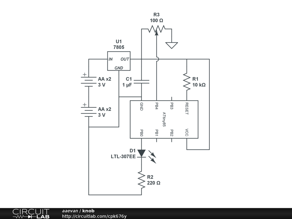
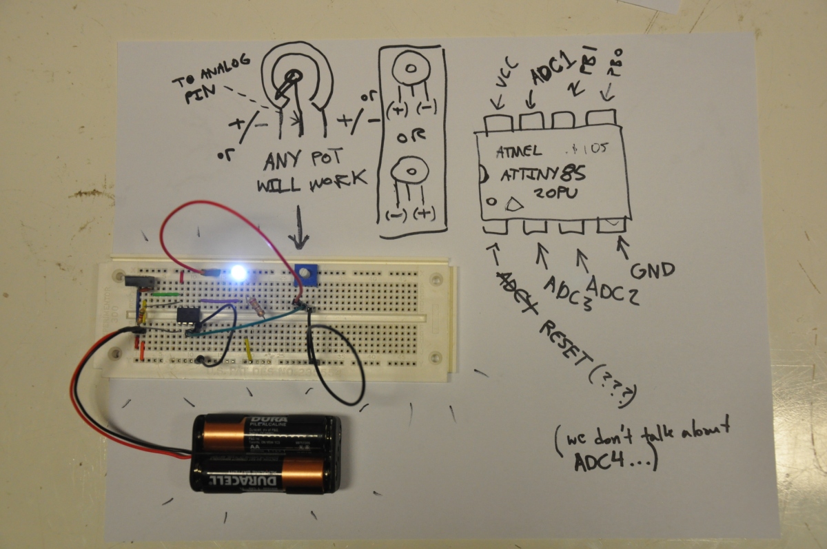
Components
Knob builds upon the blink sketch as the indicator light is still in place. Adding a potentiometer is as simple as putting one side lead to ground and the other side to VCC. The middle pin goes to the analog pin. The ATtiny has 3 analog pins that don't have weird complications. There
is a way to make the reset take analog readings but I'm not quite sure how. I haven't needed to take more than 3 analog readings yet. Analog pin 2 is used in this case.
 Click on the image to see a short video of
 knob
in action
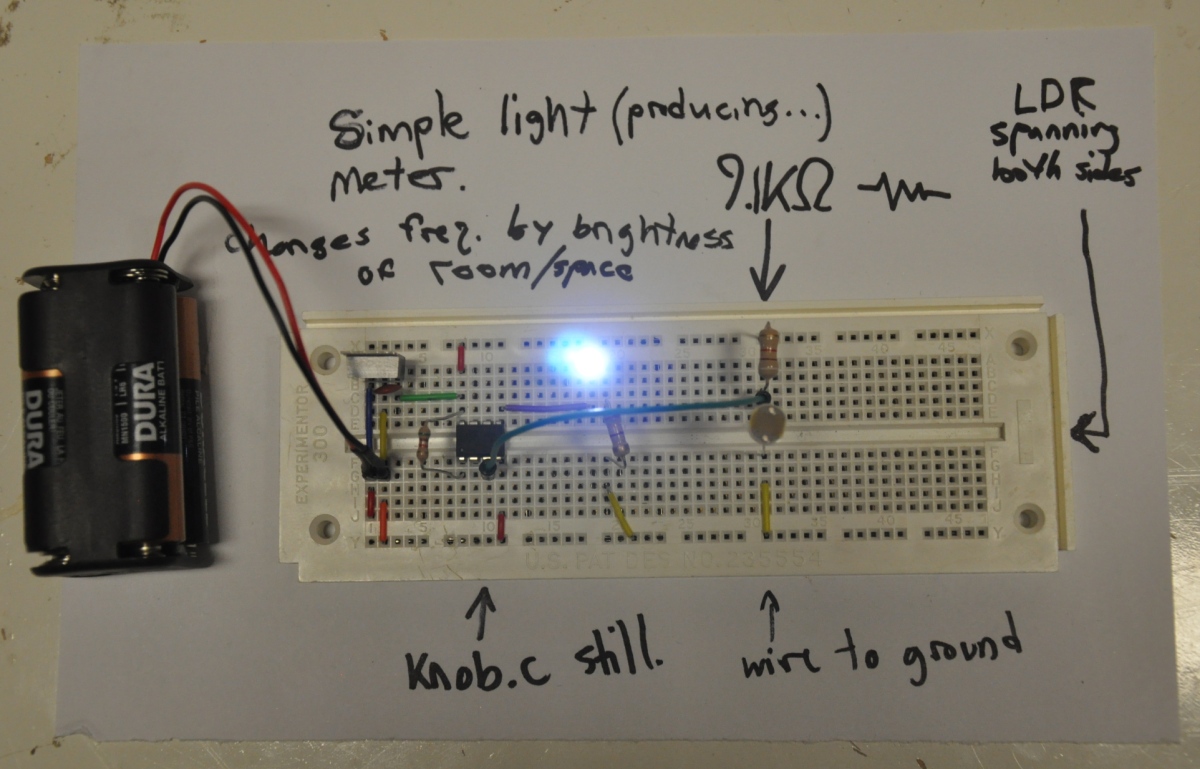
Using an LDR or other 2 pin variable resistor
Using the same code but a few different components, we can measure light levels:
(open video on click)
Next...
Now, we have the pieces to do a lot of cool things. The next section will show off some of the things I've made.

![[paper clip]](/courses/source/wiki_images/paper_clip_tilt.png)